- 您现在的位置:买卖IC网 > Sheet目录114587 > 550MH166M628DGR (SILICON LABORATORIES) VCXO, CLOCK, 166.628 MHz, LVPECL OUTPUT
Si550
2
Rev. 0.6
1. Electrical Specifications
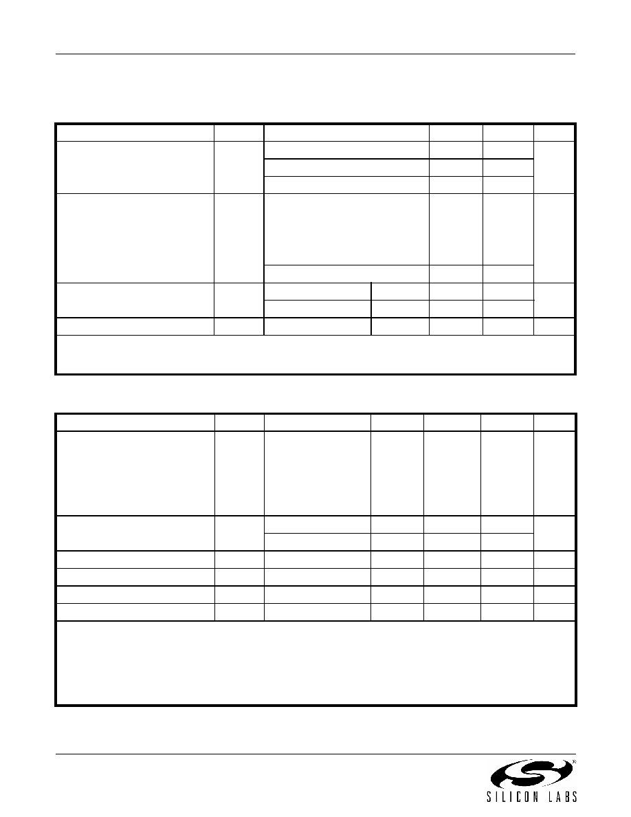
Table 1. Recommended Operating Conditions
Parameter
Symbol
Test Condition
Min
Typ
Max
Units
Supply Voltage1
VDD
3.3 V option
2.97
3.3
3.63
V
2.5 V option
2.25
2.5
2.75
1.8 V option
1.71
1.8
1.89
Supply Current
IDD
Output enabled
LVPECL
CML
LVDS
CMOS
—
120
108
99
90
130
117
108
98
mA
tristate mode
—
60
75
Output Enable (OE)2
VIH
0.75 x VDD
——
V
VIL
——
0.5
Operating Temperature Range
TA
–40
—
85
°C
Notes:
1. Selectable parameter specified by part number. See 3. "Ordering Information" on page 8 for further details.
2. OE pin includes a 17 k
resistor to VDD.
Table 2. VC Control Voltage Input
Parameter
Symbol
Test Condition
Min
Typ
Max
Units
Control Voltage Tuning Slope1,2,3
KV
10 to 90% of VDD
—33
45
90
135
180
356
—
ppm/V
Control Voltage Linearity4
LVC
BSL
–5
±1
+5
%
Incremental
–10
±5
+10
Modulation Bandwidth
BW
9.3
10.0
10.7
kHz
VC Input Impedance
ZVC
500
—
k
Nominal Control Voltage
VCNOM
@ fO
—VDD/2
—
V
Control Voltage Tuning Range
VC
0VDD
V
Notes:
1. Positive slope; selectable option by part number. See 3. "Ordering Information" on page 8.
2. For best jitter and phase noise performance, always choose the smallest KV that meets the application’s minimum APR
requirements. See “AN266: VCXO Tuning Slope (KV), Stability, and Absolute Pull Range (APR)” for more information.
3. KV variation is ±10% of typical values.
4. BSL determined from deviation from best straight line fit with VC ranging from 10 to 90% of VDD. Incremental slope
determined with VC ranging from 10 to 90% of VDD.
发布紧急采购,3分钟左右您将得到回复。
相关PDF资料
550ND125M000DGR
VCXO, CLOCK, 125 MHz, LVDS OUTPUT
550CJ153M600DGR
VCXO, CLOCK, 153.6 MHz, CMOS OUTPUT
550EJ100M000DG
VCXO, CLOCK, 100 MHz, LVPECL OUTPUT
550EK100M000DGR
VCXO, CLOCK, 100 MHz, LVPECL OUTPUT
550GD050M000DGR
VCXO, CLOCK, 50 MHz, CMOS OUTPUT
550PC061M440DG
VCXO, CLOCK, 61.44 MHz, CMOS OUTPUT
550PG065M000DGR
VCXO, CLOCK, 65 MHz, CMOS OUTPUT
550CE19M4400DG
VCXO, CLOCK, 19.44 MHz, CMOS OUTPUT
相关代理商/技术参数
550MJ300M000DG
功能描述:VCXO振荡器 Single VCXO 7mmx5mm 6 pin RoHS:否 制造商:Fox 封装 / 箱体:5 mm x 3.2 mm 频率:19.2 Mhz 频率稳定性:2.5 PPM 输出格式: 封装:Reel 电源电压:3 V 端接类型:SMD/SMT 尺寸:3.2 mm W x 5 mm L x 1.5 mm H 最小工作温度:- 20 C 最大工作温度:+ 75 C
550MJ409M600DG
制造商:Silicon Laboratories Inc 功能描述:OSCILLATOR - Trays
550MJ64M1520DGR
制造商:Silicon Laboratories Inc 功能描述:VCXO, 64.1520000MHZ, LVPECL, 3.3V - Tape and Reel
550MM400M000DG
制造商:Silicon Laboratories Inc 功能描述:OSCILLATOR - Trays
550MM400M000DGR
制造商:Silicon Laboratories Inc 功能描述:OSCILLATOR - Tape and Reel
550MM491M520DG
制造商:Silicon Laboratories Inc 功能描述:CONTROLLED OSCILLATOR 491.52MHZ VCXO LVPECL 6-PIN SMD - Trays
550MM491M520DGR
制造商:Silicon Laboratories Inc 功能描述:CONTROLLED OSCILLATOR 491.52MHZ VCXO LVPECL 6-PIN SMD - Tape and Reel
550MM912M000DG
功能描述:VCXO振荡器 SINGLE VCXO 6 PIN 0.5PS RS JTR RoHS:否 制造商:Fox 封装 / 箱体:5 mm x 3.2 mm 频率:19.2 Mhz 频率稳定性:2.5 PPM 输出格式: 封装:Reel 电源电压:3 V 端接类型:SMD/SMT 尺寸:3.2 mm W x 5 mm L x 1.5 mm H 最小工作温度:- 20 C 最大工作温度:+ 75 C